- 您现在的位置:买卖IC网 > Sheet目录511 > SI5040-D-GM (Silicon Laboratories Inc)IC TXRX XFP 10GBPS 32LGA
�� �
�
�Si5040�
�10.2.� SPI-Like� Interface�
�When� configured� in� SPI-like� control� mode� (pin� SPSEL� tied� high),� the� control� interface� to� the� Si5040� is� a� 3-wire�
�interface� modeled� close� to� commonly-available� microcontrollers� and� bidirectional� serial� peripheral� devices.� The�
�interface� consists� of� a� clock� input� (SCK),� slave� select� input� (SS),� and� serial� data� input/output� (SD).� The� SD� pin� may�
�be� configured� as� a� CMOS� output� or� as� an� open� drain� output� using� Register� 2,� bit� 4.�
�Data� is� transferred� one� byte� at� a� time,� with� each� register� access� consisting� of� a� pair� of� byte� transfers.� Figure� 7� and�
�Figure� 8� on� page� 15� illustrate� read� and� write/set� address� operations� on� the� SPI� bus,� and� Table� 9� on� page� 14� gives�
�the� timing� requirements� for� the� interface.� Table� 12� shows� the� SPI� command� format.�
�The� first� byte� of� the� pair� is� the� instruction� byte.� The� "Set� Address"� command� writes� the� 8-bit� address� value� that� will�
�be� used� for� the� subsequent� read� or� write.�
�The� "Write"� command� writes� data� into� the� device� based� on� the� address� previously� established,� and� the� "Write/�
�Address� Increment"� command� writes� data� into� the� device� and� automatically� increments� the� register� address� for�
�use� on� the� subsequent� command.� The� "Read"� command� reads� one� byte� of� data� from� the� device,� and� the�
�"Read/Address� Increment"� reads� one� byte� and� increments� the� register� address� automatically.�
�The� second� byte� of� the� pair� is� the� address� or� data� byte.� As� shown� in� Figure� 7� and� Figure� 8� on� page� 15,� SS� should�
�be� held� low� during� the� entire� two� byte� transfer.� Raising� SS� resets� the� internal� state� machine;� so,� SS� must� be� raised�
�between� each� two� byte� transfers� to� guarantee� that� the� state� machine� will� be� reinitialized.�
�During� a� read� operation,� the� SD� becomes� active� on� the� falling� edge� of� SCK,� and� the� 8-bit� contents� of� the� register�
�are� driven� out� MSB� first.� The� SD� is� high-impedance� on� the� rising� edge� of� SS.� During� write� operations,� data� is�
�driven� into� the� Si5040� via� the� SD� pin� MSB� first.� Data� always� transitions� with� the� falling� edge� of� the� clock� and� is�
�latched� on� the� rising� edge.�
�The� clock� should� return� to� a� logic� high� when� no� transfer� is� in� progress.� The� Si5040� SPI-like� interface� supports�
�continuous� clocking� operation� where� SS� is� used� to� gate� two� byte� transfers.�
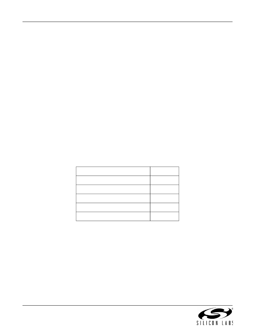
�Table� 12.� SPI-Like� Command� Format�
�Instruction�
�00000000—Set� Address�
�01000000—Write�
�01100000—Write/Address� Increment�
�10000000—Read�
�10100000—Read/Address� Increment�
�Address/Dat�
�AAAAAAAA�
�DDDDDDDD�
�DDDDDDDD�
�DDDDDDDD�
�DDDDDDDD�
�36�
�Rev.� 1.3�
�发布紧急采购,3分钟左右您将得到回复。
相关PDF资料
SI5402DC-T1-GE3
MOSFET N-CH D-S 30V 1206-8
SI5403DC-T1-GE3
MOSFET P-CH 30V 6A 1206-8
SI5432DC-T1-GE3
MOSFET N-CH 20V 6A 1206-8
SI5440DC-T1-GE3
MOSFET N-CH D-S 30V 1206-8
SI5441DC-T1-GE3
MOSFET P-CH D-S 20V 1206-8
SI5443DC-T1-GE3
MOSFET P-CH D-S 20V 1206-8
SI5468DC-T1-GE3
MOSFET N-CH D-S 30V 1206-8
SI5475BDC-T1-GE3
MOSFET P-CH 12V 6A 1206-8
相关代理商/技术参数
SI5040-D-GMR
制造商:Silicon Laboratories Inc 功能描述:XFP Transceiver 1TX 1RX 10Gbps 32-Pin LGA T/R 制造商:Silicon Laboratories Inc 功能描述:XFP TRANSCEIVER, PB FREE - Tape and Reel 制造商:Silicon Laboratories Inc 功能描述:IC TXRX XFP 10GBPS 32LGA
SI5040-D-ZM2
制造商:Silicon Laboratories Inc 功能描述:XFP TRANSCEIVER, PB FREE - Rail/Tube
SI5040-D-ZM6
制造商:Silicon Laboratories Inc 功能描述:XFP TRANSCEIVER - Rail/Tube
SI5040-D-ZM7
制造商:Silicon Laboratories Inc 功能描述:XFP TRANSCEIVER, PB FREE - Rail/Tube
SI5040-EVB
功能描述:BOARD EVAL SI5040 RoHS:否 类别:编程器,开发系统 >> 评估演示板和套件 系列:- 产品培训模块:Obsolescence Mitigation Program 标准包装:1 系列:- 主要目的:电源管理,电池充电器 嵌入式:否 已用 IC / 零件:MAX8903A 主要属性:1 芯锂离子电池 次要属性:状态 LED 已供物品:板
SI5041-B-GM
制造商:Silicon Laboratories Inc 功能描述:10G DUAL CDR (REV B FOR PROTOTYPE ONLY, REV C FOR P - Rail/Tube
SI5041-B-GMR
制造商:Silicon Laboratories Inc 功能描述:10G DUAL CDR (REV B FOR PROTOTYPE ONLY, REV C FOR P - Tape and Reel
SI5041-C-GM
制造商:Silicon Laboratories Inc 功能描述:10G DUAL CDR, LEAD FREE - Rail/Tube